Developed By:
Akshay Daga
ADC is an electronics device that converts the analog signals to digital number proportional to the magnitude of voltage. The ADC chips like ADC0804, ADC0809 etc., give 8-bit digital output. The controller device needs eight pins to receive the 8-bit data (For more details about ADC refer to Using Inbuilt ADC of AVR). Some applications need higher resolution ADCs, (10 or higher bits digital data output) for data accuracy.
Using parallel ADCs is one option for such applications. However using parallel ADC will increase the size of the hardware as a 10-bit parallel ADC will have 10 output lines. Also you might have to use controller with higher number of pins. The other option is to use serial ADC, which needs smaller number of pins. Since the data is transmitted serially, the data transfer rate of the serial ADC is low as compared to parallel ADC. They can serve as a very good alternative in applications where speed of data transfer in not a critical point. This article explores interfacing of serial ADC0831 with ATmega16.

The ADC0831 is an 8 pin, single channel serial ADC which gives 8-bit data output. The input can be either single ended or differential type. Using the differential input option, A/D conversion can be performed for two different voltage levels. The function of each pin is described in the following table:

Fig. 2: Pin Name and Fuctions of serialADC0831
1. (Chip Select) – In order to initiate conversion a high-to-low is provided on.
2. Vin (+) (Positive Analog Input) - Positive voltage is applied at this pin. The input range for this is 0 to 5votls.
3. Vin (-) (Negative Analog input) - Negative voltage is applied at this pin.
4. GND (Ground) - This pin is connected to the ground of circuit.
5. Vref (Reference Voltage) – This pin is used to set the input voltage range of ADC.
6. CLK (Clock) - Clock pulse is provided on CLK pin for synchronization.
7. DO (Data Output) - This pin is an output pin of ADC, serial output data is available on this pin.
8. Vcc (Power Supply) - This is connected to +5 volt power supply.
How serial ADC works:

Fig. 3: Block Diagram of Serial ADC Working with AVR
The above diagram shows a system in which the ADC device receives analog data from transducer. The controller is used to control ADC IC and to process the converted digital data. The analog signal is given at pin Vin(+). In differential mode, voltage at pin Vin(+) must be greater than Vin(-) otherwise output data will not be generated by the ADC. The data conversion is started by giving high to low pulse at the CS pin. At the first clock cycle, the ADC sends ‘0’ bit to the controller which shows the following bits are the data bits. The MSB of converted data is sent first. The timing diagram of ADC0831 is shown below.

Fig. 4: Timing Diagram of ADC0831 for serial communication in AVR
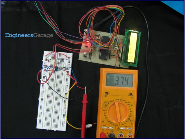
Objective: To convert analog output voltage of variable resistor into digital signals using ADC0831 and display it on LCD.
Circuit description:
The connection of ADC0831 with ATmega16 is shown in the circuit diagram. The output of variable resistor is connected to Vin(+) and Vin(-) pin is grounded. The Pins CS, CLK and DO of ADC are connected to microcontroller.
Programming steps:
1. Send a high to low pulse to CS pin to initialize conversion.
2. Monitor the status of D0 bit until it goes low.
3. Send a clock pulse.
4. Receive the data bits from DO pin of ADC 0831.
5. Store the data bits in a variable by using bitwise operation.
6. When the data byte is received from serial ADC, display it on LCD.
Circuit:
Code:
// Program to interface serial ADC 0831 with AVR microcontroller (ATMEGA 16)
#include<avr/io.h>
#include<util/delay.h>
#include<inttypes.h>
#define DO PD2
#define CLK PD1
#define CS PD0
#define lcdport PORTA
#define rs PB0
#define rw PB1
#define en PB2
void lcd_init(void);
void lcdcmd(unsigned char);
void lcddata(unsigned char);
void adc_conversion(unsigned char);
void twi_init();
unsigned char adc_read();
int main()
{
unsigned char data[12]= "ADC OUTPUT:";
int i=0;
unsigned char bits=0;
DDRA=0xFF;
DDRB=0x07;
DDRD=~_BV(DO); //DO pin is input pin and rest of the pins are output pins
DDRC=0xFF;
PORTD=0x07;
lcd_init();
while(data[i]!='\0')
{
lcddata(data[i]);
_delay_ms(5);
i++;
}
while(1)
{
PORTD|=(1<<CS); // high-to-low pulse is provided to CS pin
_delay_ms(1);
PORTD&=~(1<<CS);
_delay_ms(1);
while(PIND & _BV(DO)) // wait until 0 bit is received
{
PORTD|=(1<<CLK);
_delay_ms(1);
PORTD&=~(1<<CLK);
_delay_ms(1);
}
PORTD|=(1<<CLK); // a clock pusle is provided
_delay_ms(1);
PORTD&=~(1<<CLK);
_delay_ms(1);
for(i=0;i<8;i++)
{
PORTD|=(1<<CLK); // data receive when pulse is high
_delay_ms(1);
bits=bits<<1; //"bits" is variable to store data.left shift operation is perform to make place for upcoming bit
if(bit_is_set(PIND,DO)) // if 1 is received
bits |=1; // bits is increment by 1
PORTD&=~(1<<CLK); // pulse low
_delay_ms(1);
}
adc_conversion(bits); //
}
}
/* this function is written to convert interger value to their corresponding ASCII value*/
void adc_conversion(unsigned char adc_out)
{
unsigned int adc_out1;
int i=0;
char position=0xC2;
for(i=0;i<=2;i++)
{
adc_out1=adc_out%10;
adc_out=adc_out/10;
lcdcmd(position);
lcddata(48+adc_out1);
position--;
}
}
void lcd_init() // fuction for LCD initialization
{
lcdcmd(0x38);
lcdcmd(0x0C);
lcdcmd(0x01);
lcdcmd(0x06);
lcdcmd(0x80);
}
void lcdcmd(unsigned char cmdout)
{
lcdport=cmdout;
PORTB=(0<<rs)|(0<<rw)|(1<<en);
_delay_ms(10);
PORTB=(0<<rs)|(0<<rw)|(0<<en);
}
void lcddata(unsigned char dataout)
{
lcdport=dataout;
PORTB=(1<<rs)|(0<<rw)|(1<<en);
_delay_ms(10);
PORTB=(1<<rs)|(0<<rw)|(0<<en);
}


Không có nhận xét nào:
Đăng nhận xét